By leveraging the distinctive specialization in “Key Technologies for Aramid and Carbon Fiber Modification”, School of Materials Science and Engineering is fostering a strong adhesive research community that capitalizes on regional advantages. With a focus on the strength of “High-Energy Beam Manufacturing”, the School aims to transition from traditional “manufacturing” methods to innovative “smart manufacturing” practices. By tapping into the distinct specialties of “Electronic Packaging Materials and Technology”, it is creating an integrated mechanism that combines industry and education to nurture talent. School of Materials Science and Engineering, aligning with societal needs and industry trends, leverages its research strengths to facilitate the high-quality development of the School.
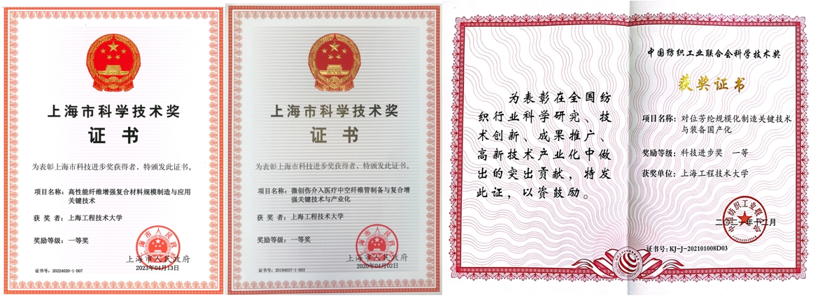
In terms of specialization, the School has focused on “key technologies for aramid and carbon fiber modification”, establishing a research team and fostering a collaborative research community with complementary strengths in adhesive technology. Over the past three years, it has been awarded two first prizes for scientific and technological progress by Shanghai Municipal Science and Technology Commission and one first prize by China Textile Industry Association. Moving forward, the School will continue to center its efforts around “Key Technologies for Fiber Material Modification”, strengthening team development through talent recruitment and training. Its goal is to achieve breakthroughs in top-tier academic papers, talent development projects, national major projects, national scientific and technological awards, and major cross-disciplinary projects.
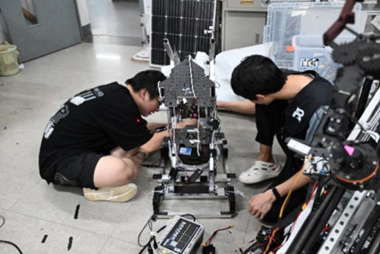
In terms of strength, the School has focused on the research of “high-energy beam connection”, gradually transitioning from “basic research” to “applied research”. This shift has expanded its focus from a single point to a comprehensive chain, thereby establishing a distinct research strength. Particularly noteworthy are the significant breakthroughs made in the fundamental research of “New Mechanisms for Interface Regulation in High-Energy Beam Connection of Heterogeneous Materials”. Over the past two years, it has garnered two second prizes in natural science from provincial and ministerial levels, as well as one second prize for technological progress from the Mechanical Industry Association. This direction leverages one “Class III” peak discipline, two provincial and ministerial-level research platforms, and one double-certified laboratory, continually enhancing the research influence in the field of high-energy beam connection. Looking ahead, the “strength” chain will be further extended to “Surface Modification of High-Energy Beams”. In this field, the School’s research is not only early and foundationally solid but also distinctly featured, yielding abundant results and possessing significant influence and competitiveness domestically. Building upon the current emphasis on academic and technical research, the School aims to expand towards multidimensional directions, integrating “academics + technology + equipment” to achieve the transformation from high-energy beam “manufacturing” to “smart manufacturing”.
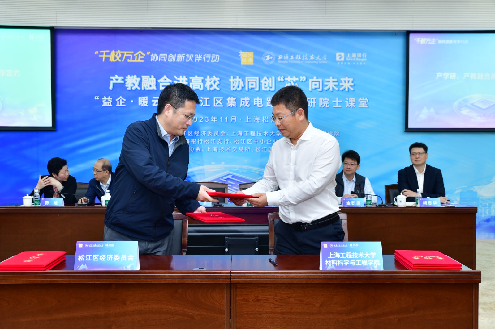
In terms of specialty, in response to the call for the key development of the integrated circuit industry chain by the nation and Shanghai, the School has been proactive in establishing the undergraduate program of Material Forming and Control Engineering (Microelectronic Packaging). It has become one of the earliest institutions in the country to offer this program, establishing a unique presence in the field of electronic packaging technology. Building on this specialized program, the School continuously explores new models for talent cultivation that align with industry demands, gradually developing a high-level engineering application-oriented talent cultivation system for the integrated circuit industry, thereby nurturing distinct strengths.
Focusing on talent development as its core mission, the School has expanded into the research field of “electronic packaging materials and technology”, significantly enhancing its capabilities in scientific research and societal contribution. Building on its strength, the School has cultivated its unique specialty. Since 2007, it has secured 49 grants from the National Natural Science Foundation, with 13 allocated to “Electronic Packaging Materials and Technology”, representing 27% of the total. Looking ahead, the School will continue its emphasis on “Electronic Packaging Materials and Technology”, shouldering the responsibility for national and regional economic growth. It aims to seamlessly integrate the School's development into the national strategic framework for the integrated circuit industry, while also aiming to align its program development with international technological advancements in this field. Additionally, it plans to establish a comprehensive talent development model spanning the entire industry chain, ensuring that talent cultivation is seamlessly integrated into all aspects of the national integrated circuit industry.
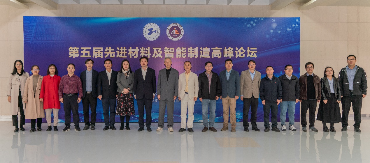
In the next phase, the School will prioritize the development of three key areas: Key Technologies for Aramid and Carbon Fiber Modification, High-Energy Beam Connection (Material Connection Interface Regulation Mechanism), and Electronic Packaging Materials and Technology. This endeavor aims to establish disciplines with distinct characteristics, excel in research expertise, provide effective services, and achieve high-level accomplishments.